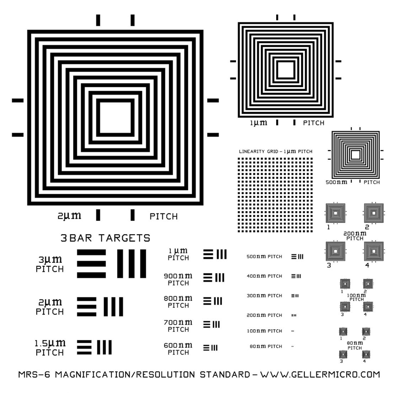
Pattern Design
The MRS-6 is fabricated by using the highest accuracy electron direct write
semiconductor manufacturing equipment available today. The pattern is built on a
silicon wafer with a 15nm Cr film. This film, which is significantly thinner that
that of the MRS-5 has superior edge quality. Imaging contrast in both secondary
and backscattered electron mode is possible with field emission SEMs and newer
tungsten or LaB6 SEMs. The overall size is ~ 3.2mm X 3.2mm X 0.5 mm thick.
The MRS-6 is fully conductive. No coatings are required or desirable. The
standard can be cleaned using a low power plasma etcher with oxygen gas.
The geometric design of the MRS-6 and MRS-5 are the same. There are three
different types of patterns.
-
Groups of nested squares spanning several orders of magnitude with
pitches of 80nm, 100nm, 200nm, 500nm, ½µm, 1µm, and 2µm.
To allow for more testing the 80, 100 and 200nm patterns are repeated four times.
-
incorporated into the standards is an extension of the 1951 USAF 3-bar
targets. These finer patterns have pitches ranging from 80nm to 3µm in
15 steps. They will find good use measuring the resolution of state-of-the-art
optical microscopes (UV, confocal, laser scanning, etc.
-
The ½µm square test pattern will help analyze your images for all
types of dimensional distortions, vibrations and magnetic fields. This
pattern contains ½µm squares with a 1µm pitch over a 20µm X and Y
field.
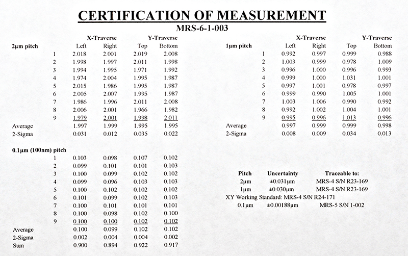
Measured and certified are pitches (the distance between repeating parallel lines using
center-to-center or edge–to-edge spacing). These are the only type of
measurements that can be used to relate measurements from different microscopy
techniques (see "Submicrometer Linewidth Metrology in Optical Microscopy",
Nyysonen & Larrabee, Journal of the Research of the National Bureau of
Standards, Vol. 92, No. 3, 1987). Linewidth measurements (the measurement of a
single line or space width) can only be related if the same type of illumination is
used as for the calibrating instrument since edge effects lead to uncertainty in the
edge locations. Using pitch measurements, errors from edge-to-edge locations
cancel as long as like positions are measured.
Square boxes and the 1µm pitch square test patterns are used for measuring
magnification simultaneously in the X and Y directions. This gives a measure of
image skew, barreling, pincushion and other non-linearity's which can have
various origins, such as from stray magnetic fields. With the MRS-6 we have
provided a large range of pitches to closely match the needs of your
instrumentation.
The largest pattern has an overall dimension of 40µm square. It contains lines and
spaces that are nominally 1µm wide. This can be used to check magnifications
greater than 1,000X. The smaller patterns allow calibrations up to 1,000,000X.
The 3-bar targets were included as a response to many requests for a standard
capable of measuring resolving power for patterns smaller than the 1951 USAF
targets.
They are often found covering a range of 0.25 to 228 cycles/mm. The standard target
element consists of two patterns (two sets of lines) at right angles to each other.
Each consists of three lines separated by spaces of equal width. The bar length to
width ratio is 5X. The patterns change size exponentially in groups and elements.
The range in line length for the original target was from 10mm to 0.08769mm.
Others have expanded the range towards finer patterns. We now extend the range
to a line width of 0.00004mm! With these 15 patterns measurement of modulation
transfer functions is made much simpler.
The patterns can also be used for determining imaging and chemical spatial resolution and chemical mapping.
|
Pattern
|
Pitch Spacings
|
Nested
boxes |
2µm |
1µm |
500nm |
200nm
4 each |
100nm
4 each |
80nm
4 each |
3 bar
targets |
3µm |
2µm |
1µm |
1.5µm |
1µm |
900nm |
3 bar
targets
continued |
800nm |
700nm |
600nm |
500nm |
400nm |
300nm |
3 bar
targets
continued |
200nm |
100nm |
80nm |
|
|
|
Traceability
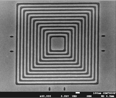
Scanning electron microscope, 80nm pitch
(in-lens secondary electrons)
|
|
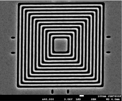
Scanning electron microscope, 80nm pitch
(type I secondary electrons)
|
Why should you consider a traceable standard? Beyond the requirements of
national and international quality standards, purchasing a CRM (certified
reference material) from a national laboratory or a traceable standard from a
certifying body (such as Geller MicroÅnalytical Laboratory) guarantees
dimensions. Most commercially available standards have unknown accuracies.
Measurements determined by optical methods measuring pattern frequency do
not tell you about the individual variations in pitch measurements- and this is
what you image. The MRS-6 is offered with or without traceability. The nontraceable
standard differs only in documentation and cost. Traceability in the X
and Y dimensions is established from a MRS-5 that has been measured by NPL
(National Physics Laboratory), the NIST counterpart in the U.K. We are in the
process of having the MRS-6 measured by a national laboratory and expect
measurements with lower uncertainties. The non-accumulative 2σ pitch
uncertainty is ±3 nm. Through international agreements our ACLASS
accreditation provides equivalency with NAVLP and A2LA. See
http://www.gellermicro.com/quality_control/QC.html.
Through national laboratory mutual recognition agreements NPL measurements are equivalent to NIST.
Traceable measurements are only provided for the 2, 1 and 0.1 μm pitch patterns.
Details can be found on the provided measurement certificates.
Recertification Program
We are often asked why the MRS needs re-certification. Under ISO-17025
guidelines, your quality department should determine the re-certification interval
as they are most familiar with your company's quality system requirements.
Recertification is a common practice for devices such as gage blocks and electronic
instruments. Over the years we have found several standards which could not be
recertified due to physical damage and excessive contamination. In a few cases
we have seen electron beam damage and corrosion from storage in a
contaminating environment. Re-certification insures your standard will perform
its proper task and that you will be meeting your quality system directives.
Recertification includes cleaning.
Magnification Measurements
Optical Microscope magnifications can be measured only in the reflection
mode by directly on viewing CRTs, in reticles mounted within the ocular, or
directly on photomicrographs. Please note the contrast is not particularly high.
For instruments with verniers or electronic calipers distance measurements can
be verified using a pitch pattern of appropriate size. Magnification is simply the
image size divided by the object size (be careful to use the same units).
Scanning Electron Microscopes and FIB/SEMs can use the secondary electron signal at an
accelerating voltage of <=25keV preferably with type II secondary electrons to
get more of a surface image. Backscattered electron imaging is possible but only
for high sensitivity detectors.
To avoid pattern damage use <1 nA electron beam current.
Scanning Probe Microscope operators must be aware of the fine dimension of
the pitch patterns. The 80nm pitch has a nominal space width of 40nm. The
cantilever tip must be smaller to define the pattern. As shown in the AFM image
to the left the pattern lines have variable height.
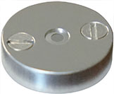
Retainer & Mounting Options for SEM
|
|
The MRS-6 Calibration Standard comes unmounted to give the customer the flexibility to mount the
standard on the position or stub they wish.
We offer two retainer & mounting options; MRS-6 on either Ø1/2" (12.7mm)
pin stub or Ø15mm Hitachi mount. These mounting options have to be ordered additional
to the MRS-6 at the time of ordering.
MRS-6 Product Ordering Information
|
International Calibration Standards
- ASTM E766–2003: Standard Practice For Calibrating The Magnification Of A Scanning Electron Microscope
- ISO 16700:1994 MICROBEAM ANALYSIS — Scanning Electron Microscopy — Guidelines For Calibrating Image Magnification
- There are no international standards for SPM magnification calibration at this time