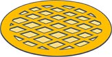
Substratek™ TEM Substrates are ultrathin metallic support films on standard 3mm TEM grids. These metallic films are specially manufactured with a patented process (US Patent #7348570 B2, March 25, 2008) as experimental platforms and are electron transparent to allow for imaging using a TEM. The ultrathin Substratek™ TEM Substrates enable electrochemical processing, crystal growth, and nano- and micro-fabrication directly on the substrates. They allow for subsequent TEM examination without the need for extensive sample preparation. Direct nanoscale imaging without extensive TEM preparation does not require expensive thinning tools, it saves time and it avoids introduction of preparation artifacts. Compared to the widely used carbon support films, ultrathin and electron transparent metallic films have a high surface energy and therefore more suitable for fabrication processes.
Important properties of the ultrathin Substratek™
Metallic Support Films are:
- Electron transparent with a 2-3nm thickness
- Small feature sizes do not obscure sample features
- Chemically stable (can be used for electroplating)
- Robust enough to act as substrates
- High surface energy.
They are ideally suited for use as integrated research
platforms for applications as diverse as:
- Nanofabrication
- Electron-beam lithography
- Micro-contact printing
- Electrochemistry or electroplating
- Nano-crystal growth
- Carbon nano tubes
- X-ray analysis of carbon containing materials
- Surface and interface science
|
|
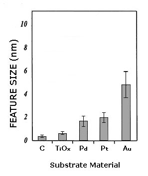
The Substratek™ TEM Substrates are metallic ultrathin films on a standard 3mm TEM grid. Available substrate are Au, Pt, Pd (2-3nm thickness) and TiOx (10-20nm thickness) on 300 and 400mesh TEM grids. The Au, Pt and Pd substrates are deposited on gold TEM grids compatible with electrochemical processes. The TiOx substrate is deposited on copper TEM grids; These materials have proven to be stable substrates with a small feature size in the support film. The TiOx substrate is more bio-compatible and can also be used for life-science applications. They are supplied in a PELCO® 160 TEM grid box in quantities of 25 per box.
References:
- Daniel B Allred, Melvin T. Zin, Hong MA, Mehmet Sarikaya, Francois Baneyx, Alex K.Y. Jen, Daniel T. Schwartz, "Direct nanofabrication and transmission electron microscopy on a suite of easy-to-prepare ultrathin film substrates", Thin Solid Films, 515(13): 5341 - 5347, 2007
- Daniel B. Allred, Anchi Cheng, Mehmet Sarikaya, Francois Baneyx, Daniel T. Schwartz, "Three-dimensional architecture of inorganic nanoarrays electrodeposited though a surface-layer protein mask", Nano Letters, 8 (5): 1434 - 1438, 2008
- Yusuke Ominami, Quoc Ngo, Makoto Suzuki, Alexander J. Austin, Carry Y. Yang, Alan M. Cassell, Jun Li, "Interface
characteristics of vertically aligned carbon nanofibers for interconnect applications", Applied Physics Letters, 89 :
263114 (1-3), 2006
Technical Notes (PDF 79KB)
TEM substrates on 400 mesh TEM grids
G400: Pitch 62µm; Hole Width 37µm; Bar Width 25µm; Transmission 37%
| Prod #
| Description
| Unit
| Price
| Order / Quote
|
| 21410-25
| Substratek™, 2-3nm Pt on 400 mesh Au TEM grid
| pkg/25
| $99.60
|
|
| 21420-25
| Substratek™, 2-3nm Au on 400 mesh Au TEM grid
| pkg/25
| 99.60
|
|
| 21430-25
| Substratek™, 2-3nm Pd on 400 mesh Au TEM grid
| pkg/25
| 99.60
|
|
| 21440-25
| Substratek™, 10-20nm TiOx on 400 mesh Cu TEM grid
| pkg/25
| 99.60
|
|
TEM substrates on 300 mesh TEM grids
G300: Pitch 83µm; Hole Width 58µm; Bar Width 25µm; Transmission 49%
| Prod #
| Description
| Unit
| Price
| Order / Quote
|
| 21310-25
| Substratek™, 2-3nm Pt on 300 mesh Au TEM grid
| pkg/25
| $99.60
|
|
| 21320-25
| Substratek™, 2-3nm Au on 300 mesh Au TEM grid
| pkg/25
| 99.60
|
|
| 21330-25
| Substratek™, 2-3nm Pd on 300 mesh Au TEM grid
| pkg/25
| 99.60
|
|
| 21340-25
| Substratek™, 10-20nm TiOx on 300 mesh Cu TEM grid
| pkg/25
| 99.60
|
|
Additional Information on Au, Pt, Pd and TiOx Substrates
Gold
Gold is an electron dense material and has relatively large background features
(similar to silver). However, gold is one of the most studied materials and is often
used for comparison. Au substrates are also often used in material science studies.
The 2nm thin Au substrate is sufficiently electron transparent to enable TEM examinations.
|
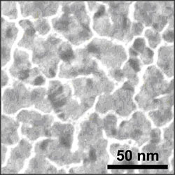 Au substrate, 2nm. Au substrate, 2nm.
|
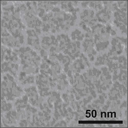
Platinum
Platinum, though a 3rd row transition metal, forms such small grain sizes that
a thin film is surprisingly electron transparent and yet still has good conductivity.
A good substrate to work with and quite robust. Useful for catalyst studies.
|
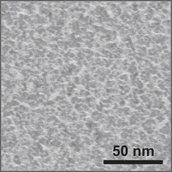 Pt substrate, 2nm. Pt substrate, 2nm.
|
Palladium
Palladium is an excellent substitute for platinum. It is more electron transparent
with small feature sizes, but it is less electrically conducting. Palladium is
currently being investigated as a substitute for gold in integrating circuits for its
lower price. Other research fields are catalyst studies and hydrogen storage.
|
 Pd substrate, 2nm. Pd substrate, 2nm.
|
Titania (TiOx)
The titania substrates are 10-20nm thick and have a very fine grain size.
Titania particles are used in countless applications. Both titanium and titania
(titaniumoxide) are considered biologically compatible materials and can be
incorporated into living tissue. Titanium implants are used as solid body implants.
Titania particles are used for cosmetic lotions and sunscreens. It is also widely
used in high end paints for the automotive and aerospace industry.
The titania films offer an excellent substrate to study crystal growth and interactions
of other materials with TiOx.
|
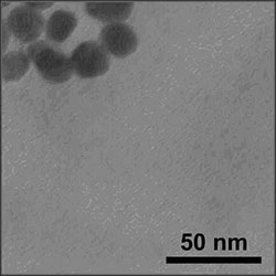 TiOx substrate, 15nm. TiOx substrate, 15nm.
Particles in the upper left corner are Au particles, used as a focusing aid.
|