Manufacturing Method
The PELCO® Silicon Dioxide Films are manufactured using the latest, patented, state-of-the-art semiconductor and MEMS manufacturing techniques. The amorphous, thermal SiO2 is grown on a 200um thick silicon wafer to the desired thickness of 40, 18 or 8nm. A 200nm silicon nitride film is grown on top of that. The specimen viewing area is created by etching away a window in the silicon substrate. Apertures are etched into the silicon nitride leaving a support mesh for the silicon dioxide. The combination of stress and compression in the two layers produce the PELCO® Silicon Dioxide Films with its superior flatness. After finishing the etching process, the individual frames with the membranes are lifted from the wafer.
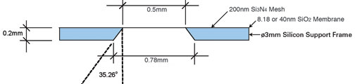
Window Sizes and Shapes
Single window of 0.5 x 0.5mm with silicon nitride support mesh creating 24 apertures. Due to the structure of the silicon and the etching process, the window in the silicon substrate is etched with a 35 angle, leaving a larger 0.78 x0.78mm opening at the back side of the frame.
40nm Membrane Thickness
18nm Membrane Thickenss
8nm Membrane Thickness
| Manufacturing Tolerances |
| Frame Thickness: |
200µm ±15µm |
|
|
| Membrane Thickness: |
40nm ±4nm |
|
18nm ±3nm |
|
8nm ±2nm |
|
|
| Mesh Thickness: |
200nm ±10nm |
|
|
| Frame Diameter: |
3.0mm ±0.05mm |
|
|
| Window Dimensions: |
500 x 500µm ±20µm |
|
Debris-free Products
Handling capabilities and smoothness of the edges are design advantages over other brands of silicon dioxide or silicon nitride support films. The PELCO® Silicon Dioxide Support Films are manufactured like TEM grids with a 3mm diameter using a unique and patented manufacturing process. They have no broken edges, are circular and the membranes are completely free from debris particles. The mechanical and thermal stability allow for cleaning or treating of the silicon dioxide support films with chemicals (solvents, acids and bases) glow discharge or plasma cleaning. It is recommended that ultrasonic cleaning is not to be used, as it can easily shatter the thin silicon dioxide support films.